
設備與零件銷售
- 全自動雙軸經原切割機
- 工業 3D CT XRAY 在線檢察機
- 全自动植片设备 (Lid Attach System)
- 點膠機
備品零件銷售
- Applied PVD Model Edurea Parts
- Bruker model JVX62 Parts
- ASML DUV parts
- TEL Parts
3D CT 工業 XRAY 檢查機
- 鋰電池快速<30 秒 3D-CT智慧檢測設備
疊片後100%CT高速全檢,漏判率0%
快速CT重建技術,3秒內實現鋰電池微米級3D/CT全掃描
單工位元節拍超12PPM,可根據產線配置至30PPM
根據尺寸自動計算檢測位置,GRR<10%
自研微焦射線源,檢測精度<5μm
高效低誤判,誤判率<1%
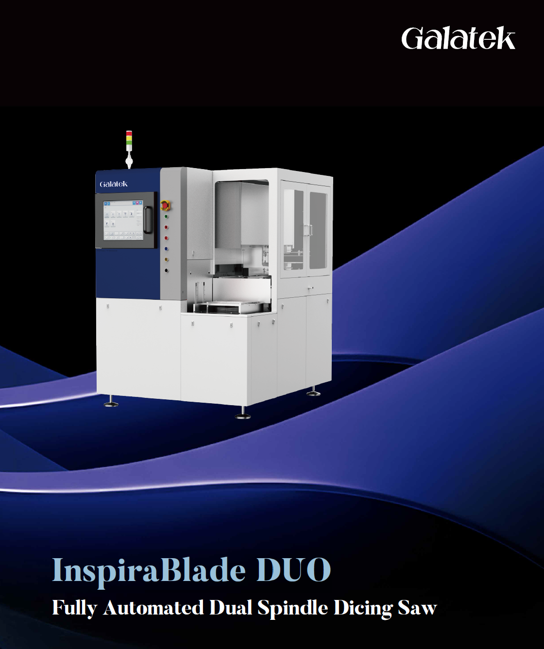
全自動雙軸切割機
Fully Automated Dual Spindle Dicing Saw
- This intelligent dicing solution is widely applicable to various wafer materials, including ceramic, silicon, glass, and lithium niobate. It also supports package saw processing scenarios involving QFN, DFN, and PCB substrates. Key features include High-resolution imaging for precise alignment, Automatic kerf inspection, BBD blade breakage detector, and NCS non-contact setup.
- Multiple functions
High-power dual spindles, multiple cutting modes
High-resolution imaging for automated precise alignment
BBD (blade breakage detector) function
NCS (non-contact setup) function
Kerf detection feature
Designed for dicing multi-type of workpiece
Cleaning function
Graphical user interface"
High production ef ciency
Stable processing quality
Length measurement alignment(CSP)
Dicing sequence and frame-removal settings
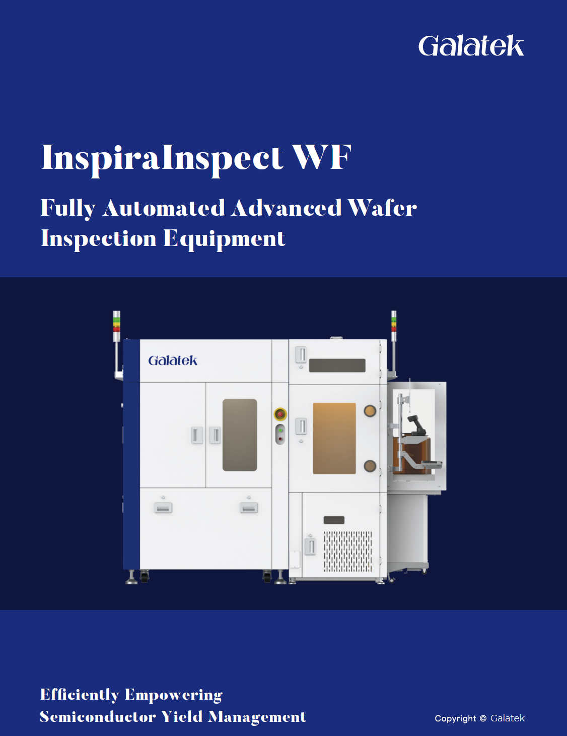
全自動晶圓片檢查設備(AOI)
Fully Automated Advanced Wafer Inspection Equipment
The Galatek InspiraInspect WF is a fully automated wafer defect inspection system engineered speci cally for appearance defect detection onpatterned wafers. It integrates both macro and micro defect detection capabilities, enabling precise identi cation of systematic and random defectsacross the wafer surface. As a core tool for semiconductor manufacturing, it plays a foundational role in wafer yield management.- Key Features
2D+AI Defect Detection:Indenti es 2D defects as small as 1 m
2D Critical Dimension (CD) Measurement: Repeatability Accuracy (3 ) ±0.1 m.
AI-powered Automatic Defect Classi cation (ADC)
High Compatibility
Comprehensive Detection Capabilities
High-performance
AI-Powered Multi-Modal Visual Inspection Solution.
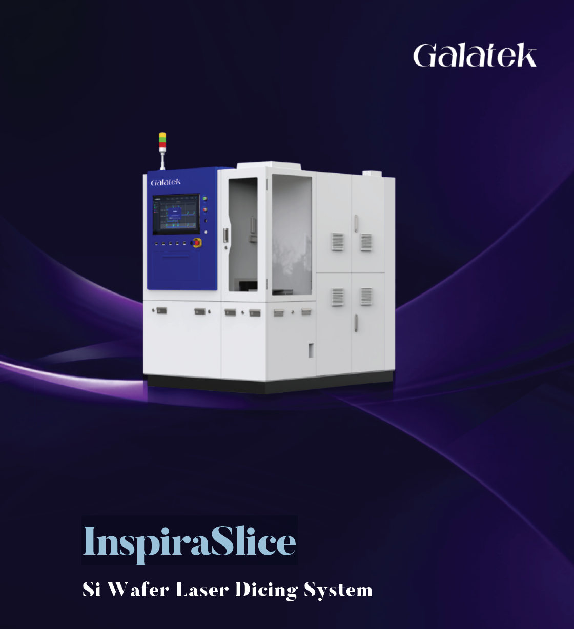
矽晶圓雷射切割系統
Si Wafer Laser Dicing System
InspiraSlice adopts advanced laser-guided cutting technology, combined with high-speed platform motion, to generate guided pre-cracks both on the surface and within silicon wafers.
Key advantages include:
- No dust contamination on the wafer surface after cutting.
- Minimal material loss.
- Small heat-affected zone.
- The system features fully automated loading/unloading, automatic image correction, precise auto-focus, real-time data statistics, and compatibility with SECS/GEM interface for seamless integration.
- Compatible wafer size.
- High precision motion platform.
- One-touch fully automated operation.
- Exceptional Dicing Accuracy.
- Industry Process Breakthrough
- Friendly interface

自動晶圓雷射開槽系統
Fully Automated Laser Grooving for Silicon Wafer.
Galatek's Fully Automated Laser Grooving System for Silicon Wafers. Engineered speci cally for the unique properties of LOW-K dielectric materials,Galatek's laser grooving solution delivers high-precision and high-ef ciency processing tailored for semiconductor applications.- Customized ultraviolet lasers—available in nanosecond, picosecond,and other short-pulse formats—support precision laser ablation processes.
- Engineered for high-ef ciency surface processing of 8″/12″ wafers with Low-k lm structures.
- Delivers fully automated, high-ef-ciency per formance with pinpoint precision and reduced thermal impact.
- Automatically applies protective coating and performs precision cleaning with high-speed spin drying.
- Key Features
One-Click Automated Operation
Superior Bottom Flatness in Grooving
Advanced Vision Platform
Dust-Free Operation
Minimal Heat-Affected Zone
SECS/GEM Protocol Compatibility
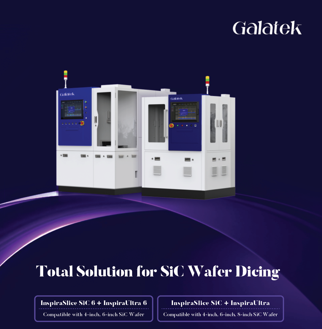
矽晶圓片切割整體解決方案
Total Solution for SiC Wafer Dicing
Silicon carbide (SiC) wafers, known for their high hardness and brittleness, often face challenges during the dicing process, such as chipping and irregular crack propagation. These issues directly reduce subsequent chip yield.
To overcome these challenges, our system provides a comprehensive SiC wafer dicing solution. It utilizes laser-guided cutting technology, focusing the laser inside the SiC wafer to create guided pre-cracks. After laser dicing further re nes these pre-cracks, the chip is separated using a three-point bending method, ensuring complete chip separation along the laser-cut lines.
Features:
- High Compatibility
- High-Precision Motion Control
- Superior Cutting Accuracy
- One-Touch Automated Production
- Industry-Leading Process Innovation
- Superior Cutting Accuracy
- User-Friendly Interface
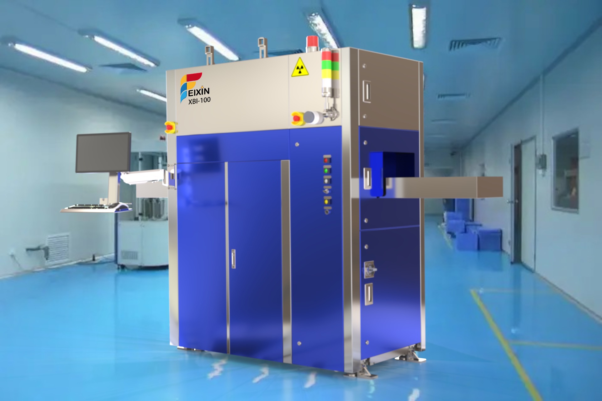
3D CT 工業 XRAY 檢查機
應用物件: 鋰離子電池 (圓柱型,軟包,方形等)
可觀察專案:
- 電極捲繞或迭層狀態
- 極片位置是否偏移
- 隔離膜縐褶或損傷
- 電解液分佈情況(若有對比劑)
- 空隙,孔洞,氣泡,脫層
3.常見缺陷:•捲繞鬆散•離子層迭不齊•異物混入(顯示為高密度區)
4.產品優勢:
- 鋰電池快速<30 秒 3D-CT智慧檢測設備
疊片後100%CT高速全檢,漏判率0%
快速CT重建技術,3秒內實現鋰電池微米級3D/CT全掃描
單工位元節拍超12PPM,可根據產線配置至30PPM
根據尺寸自動計算檢測位置,GRR<10%
自研微焦射線源,檢測精度<5μm
高效低誤判,誤判率<1%
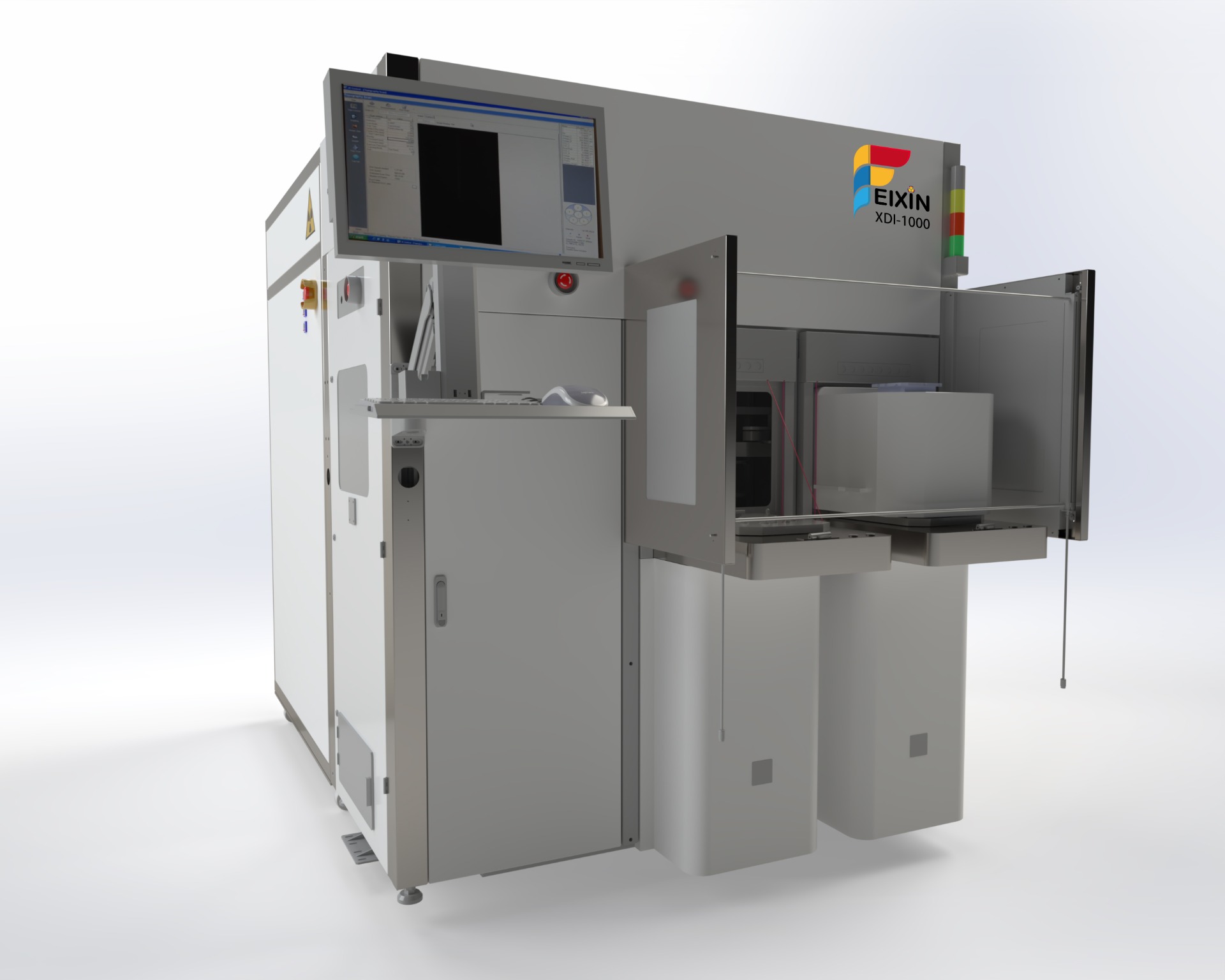
HXRD+XRR Dual channel
隨著晶片工藝邁向3nm以下節點,薄膜厚度、密度、介面粗糙度與晶體結構完整性已成為決定產品良率的關鍵。本企業推出的 X射線反射儀(XRR)與高解析度X射線衍射(HXRD)雙功能一體機,通過創新性整合兩種核心技術,實現 "單設備全維度" 工藝品質監控,為先進制程提供原子級精度的高效檢測方案。
- XRR技術:薄膜結構的"超精密尺規"
原理:通過測量X射線在薄膜表面的臨界反射角,解析薄膜厚度(精度達0.1Å)、密度(靈敏度±0.1 g/cm³)及介面粗糙度。突破性應用:超薄柵氧層、金屬柵極的厚度與密度監控低介電常數(Low-k)材料的孔隙率分析三維堆疊晶片中鍵合介面的缺陷檢測
- HXRD技術:晶體品質的"原子級探針"
原理:利用高解析度X射線衍射分析晶格應變、缺陷密度與外延層品質,精准評估溝道應力工程與異質結構可靠性。突破性應用:SiGe/Si 異質結的應變分佈映射納米鰭片(FinFET)與全環繞柵極(GAA)的晶體完整性驗證第三代半導體(如GaN-on-Si)的位元錯密度檢測
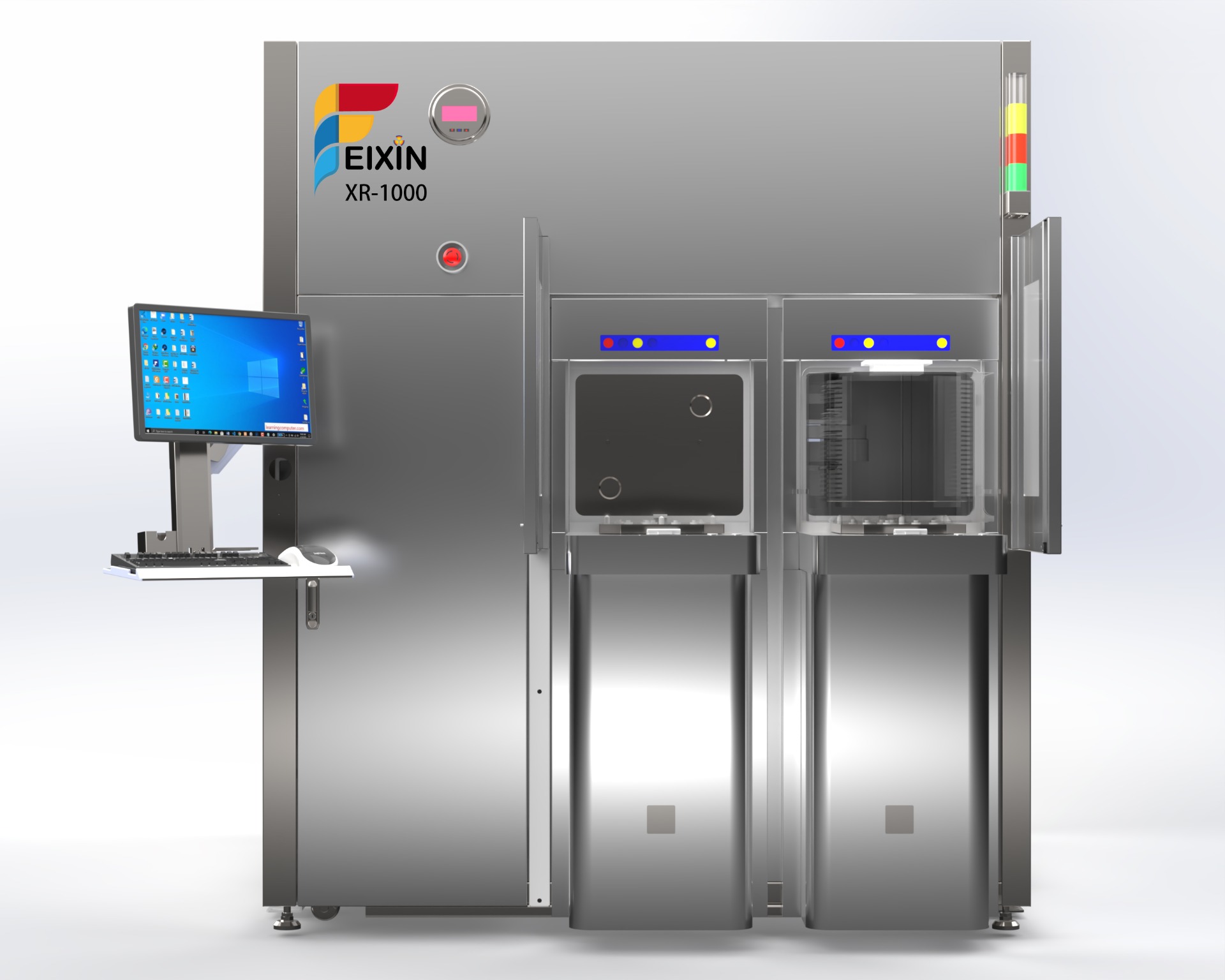
XRF X-ray Fluorescence
顛覆性技術融合:XRR與HXRD的協同賦能
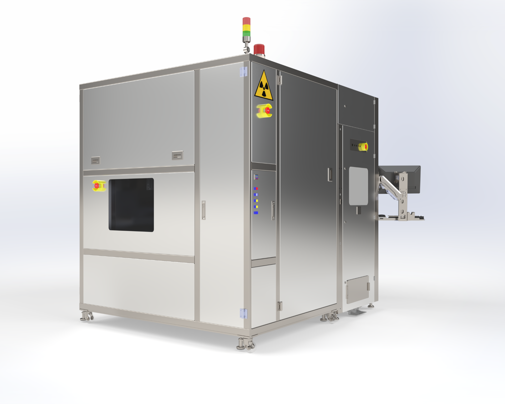
XDI X-ray defect inspection
Single-crystal diffractometer
- 點缺陷 (Point Defects)
•空位 (Vacancy):晶格中原本應有的原子位置被留空,例如離子/原子缺失。•間隙原子 (Interstitial) : 原子進入不屬於晶格位點的位置,擠入晶格孔隙中。•替代原子 (Substitutional):外來原子取代晶格中的原子位置,會引起晶格扭曲。•Frenkel 缺陷:離子離開其正常位置,形成一對空位+間隙原子。• Schottky 缺陷:陽、陰離子對成對消失,維持電中性圖中可以看到代表性的 空位 (top-left)、間隙 (top-right)、Frenkel (bottom-right)、替代 (bottom-left) 。
- 線缺陷 (Line Defects)
•邊緣位錯 (Edge Dislocation):晶粒中多出一半原子層,會影響滑移與塑性。•螺旋位錯 (Screw Dislocation):晶格部分滑移形成螺旋結構,常見於塑性變形。•面/介面缺陷 (Planar Defects)晶界 (Grain Boundary):不同晶粒間的介面,影響硬度與強度. 孿晶界、堆垛錯層 (Stacking Faults) 等會改變材料的機械/電子特性。
- 面/介面缺陷 (Planar Defects)
•晶界 (Grain Boundary):不同晶粒間的介面,影響硬度與強度•孿晶界、堆垛錯層 (Stacking Faults) 等會改變材料的機械/電子特性。
